- Heart Monitor
- Computer
- GPS technology
- File servers
- Portable phones
- Data storage
- Signal transmission
- Weather analysis
- Electricity quality testing

About the definition of a 4 layer PCB, people come up with their ideas, “As the name suggests, is a 4 layer PCB a circuit board with 4 copper layers placed?” Yes, the definition that people propose is correct. The 4 copper layers are usually 2 signal layers, one power layer, and one ground layer.
4 layer PCB takes the largest proportion of multilayer PCBs and is widely used in almost every aspect of industries, such as consumer electronics, industrial electronics, ex-communications, medical, computer, wireless, automotive, military, IoT, robotics, etc., which is the most important reason why 4 layer PCB is so widely used.
The following are some important applications where 4 layer PCBs are widely used.
How 4 layer PCB is produced, the following is a brief introduction to the production processes of 4 layer PCB:
Those who do not believe that the 4-layer PCB is very important will think like, “ There is no possibility that 4-layer PCBs are widely used in almost all kinds of electronic products.” However, such thinking is wrong. The most usually seen 4-layer PCB can be classified into the following categories:
4 layer rigid PCBs are the most widely used PCBs. The materials are usually FR4, high TG FR4, and high-speed FR4. High-frequency PCBs are made with RF material. For example, Rogers RO4350B and RO4003C are also very widely used.
Most flexible PCBs are one layer or two layers, which are used as a better substitution for cables. But flexible PCB has a smaller size and better flexibility, which can be bent thousands of times. If someone rashly says: “Flexible PCB can not be designed as a 4 layer PCB or PCB with more layers,” we will not hesitate to refute his statement.
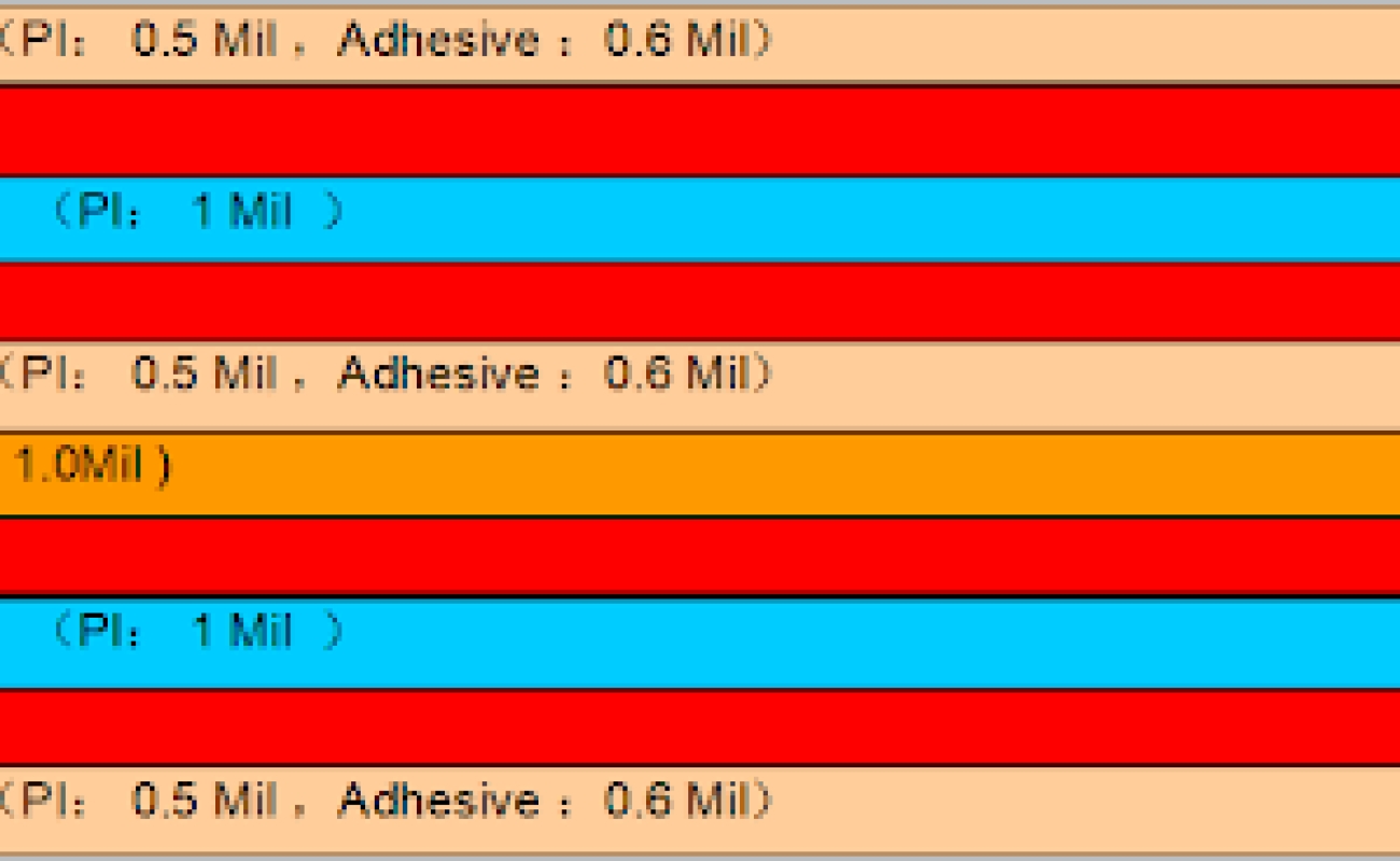
The following picture shows the most commonly used 4 layer flex PCB structure, two cores are laminated together. But normally, 4 layer flex PCB should not be used in multiple times bending situations since the thickness of 4-layer flex PCB is over 0.15mm and the flexibility is not good enough.


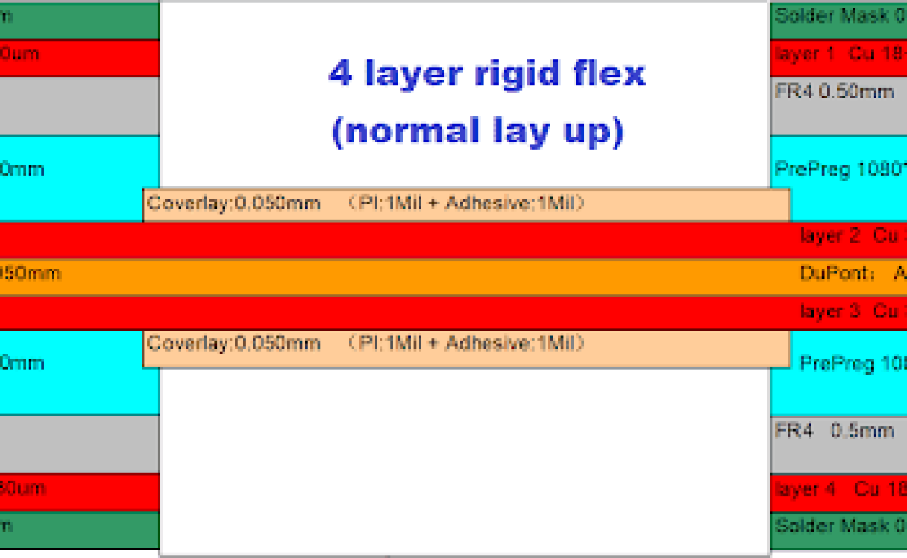
4 layer rigid-flex PCBs are normally used in cameras, drones, robotics, wearable electronics, industrial applications, etc., which need to use the advanced technology of rigid-flex PCB and also need to be cost-effective.
The normal layup of a 4-layer rigid-flex PCB is two flexible layers in the middle and two rigid layers at the top and bottom ( as in the following illustration), but the flexible layer can also be designed on the top or bottom layer. Sometimes only one flexible layer is designed.
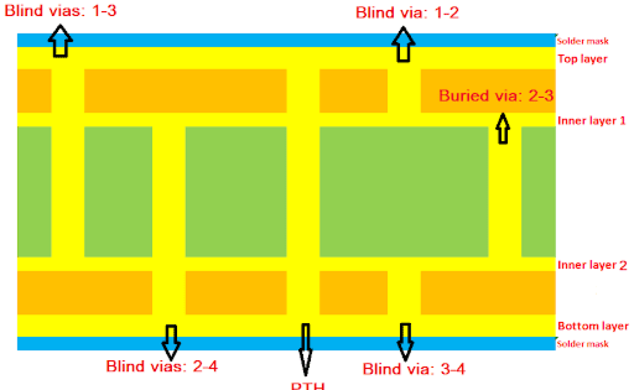
For some electronics that need very complex functions, 4 layer HDI PCB is also designed. Normally buried vias are in inner layers 2 and 3, and blind vias can be in layers 1-2, 1-3, 3-4, and 2-4.

A aluminum PCB has one copper layer usually, but sometimes can be two layers or more. 4-layer aluminum PCB is a very special 4-layer design, which is used on products that need very good thermal conductivity, and also need to assemble a lot of components.
Please contact us freely for any of your 4 Layer PCB manufacturing requirement.
About the layer structure of a 4 layer PCB, some people would say something like this, “4-layer PCB consists of the top layer, the bottom layer, and two inner layers in the middle, is that right?” Yes, such a statement is correct. As we mentioned above, usually, the top and bottom layers are signal layers, and the two inner layers are the power layer(VCC) and the ground(GND) layer. Compared with the double-sided PCB, which only has 2 layers, blind and buried holes can be designed in 4 layers of PCB, so there is more compatible space in the functionality and application of the product. Do you wonder how 4 layer PCB designers are committed to the rational design of 4 layer PCBs to achieve more functions of 4 layer PCBs? But how to design a 4-layer PCB?
Here are a few key points we should pay attention to:
Some people will ask, “Is the original design of a 4 layer PCB the same as that of a normal PCB?” They are the same.
Firstly, we should determine the compatibility and size of the PCB according to the terminal product we want to design to determine the appropriate number of layers to be designed. The number of layers can be two layers as the conventional, two layers, four layers, six layers… may be up to 40 layers or more.
After confirming the number of layers, the next step is to enter into the layout of signal points, and confirming how to divide these signal points is very important for the initial design stage. In addition, the compatibility of PCB is closely related to the stack up of PCB. If the stack up of PCB is not well designed, the electromagnetic interference of the product will be very serious, which will affect the stability of the final product.
The confirmation of stack-up is a multi-factor synthesis, not only a unilateral consideration but also a relatively perfect balance. For example, the more final layers of the PCB, the simpler the layout and distribution of the circuit and the more operable space. But relatively, the more layers, the higher the production cost. Therefore, we should consider the two together to get the perfect layers.
In addition, in stack-up, it is very important to ensure the symmetry of stacking up the structure. For the final number of layers of PCB and the final confirmation of stack up, according to Viasion’s many years of experience in PCB manufacturing, we usually determine the final number of layers of the appropriate PCB by focusing on the analysis of the signal layer and the internal electrical layer. For example, we will first complete the layout and division of components and then enter the analysis of circuits, focusing on special circuits, such as some sensitive signal lines, Take this as the core to confirm the final number of layers of the signal layer, and then come to the internal electric layer. Generally, we confirm the final number of layers of the internal electric layer based on the compatibility and stability of the power line.
Imagine that you suddenly encounter this question, “Do you agree that a 4 layer PCB usually contains two signal layers, one power layer (VCC), and one ground layer (GND)?” From the above information, we can know the answer is “Yes”. The first thing is that the signal should be adjacent to the ground and power layers, two signal layers should not be adjacent to each other, which will interfere with each other. As for the high-frequency circuit, ground and power layers should be placed in the middle, and the distance from signal layers should be as far as possible to reduce interference effectively. Digital and analog circuits shall be separated.
After confirming the number of PCB layers used in 4 layer circuit board in this step, we will enter the division of the signal layer and internal electric layer (power layer and ground layer). There are many layout modes of the signal layer and the internal layers. According to our experience, first of all, we usually make the signal layer and the internal electric layer adjacent to each other. In this way, the electromagnetic shielding ability of the signal layer can be greatly improved, and the interference ability and stability can be improved.
In addition, let’s talk about the internal electric layer in 4 layer PCB stackup design separately. We recommend reducing the thickness between the power layer and the signal layer as much as possible, which can greatly improve the capacitance between them and enhance functionality. For the thickness selection of the insulating layer, we select an appropriate thickness, usually 0.2-0.5mm. As for the signal layer, to improve the compatibility and stability of the signal layer and avoid mutual interference, it is very important not to make the signal layer adjacent.
In addition, to improve the overall compatibility and stability of 4 layer PCB boards, the high-speed signal layer should be set in the middle of the inner electric layer to form a sandwich. The inner electric layer – the high-speed signal layer – the inner electric layer. As mentioned above, the signal layer and the inner electric layer are adjacent to each other, which can greatly reduce electromagnetic radiation. The purpose of this is also to minimize the electromagnetic radiation generated by the signal layer, to greatly improve the stability and compatibility of the product, need to be noticed.
We usually ground multiple internal electric layers, which can greatly reduce the overall interference and achieve better stability. Finally, it was emphasized at the beginning that the symmetry of stack up is particularly important, and its consistency in symmetry must be guaranteed.
Please follow the above 4 layer PCB design guidelines to get a good 4 Layer PCB layout for your electronic devices.
Firstly, it is necessary to confirm the correctness of the component package, such as the size and spacing of pins. In addition, there are the size and orientation of the frame. For components with polarity, their detailed parameters should also be marked, such as number, positive and negative electrodes, etc. In addition, ensure the consistency of information, such as component information in BOM and component information in the schematic diagram. In addition, components requiring additional configuration shall be calculated according to their final combined size, such as heat sink. Then their overall package size should be the final design size. To ensure the smooth installation and assembly and the correctness of the information, for example, the pins of components should always be consistent with the inner diameter of the pad. Generally, according to Viasion’s experience, we will design a larger inner diameter of the pad.
Usually, PCB will place and arrange a large number of main components on the top layer, but there is no lack of some PCB designs that will place a large number of main components on the bottom layer, so this aspect still depends on the actual placement position of PCB components.
We usually ground multiple internal electric layers, which can greatly reduce the overall interference and achieve better stability. Finally, it was emphasized at the beginning that the symmetry of stack up is particularly important, and its consistency in symmetry must be guaranteed.
Here are some basic rules for components complacent:
The layout and routing of multi-layer boards are different from that of 1-layer and 2-layer PCB. The core point is to improve the overall anti-interference ability and stability of the circuit board by reasonably dividing the internal electric layers and adjusting the internal electric layer components. The detailed description is to reasonably classify the components.
First, the power lines should not be crossed, and the high-voltage and low-voltage power supplies should be separated. As for the angle of traces, try to ensure that the straight line is vertical. For the line that needs to be turned, 45 degrees should be adopted to form acute corners. The trace width of the connection pad should be smaller than the pad’s outer diameter. The bottom of high signal components can not go through traces, for example, crystal oscillators with high noise and transformers. The width of the power line and ground wire shall not be too small as far as possible. Otherwise, the current passing through is too large and it is easy to overload. For example, the same type of power supply should be placed together as much as possible. Although it is not the only placement condition, the components of different voltages should be placed in different categories as much as possible.
The high voltage and high voltage components should be placed together, and the low voltage and low voltage components should be placed together, and there should be a certain distance between the high and low voltage components; while ensuring these, we should also take into account the characteristics of other aspects. In addition, how to simplify the routing as much as possible? Viasion usually arranges the signal line first and then the power line. In this way, the line can be simplified as much as possible. This aims to make the power line link the internal electric layer as much as possible, reduce the interference and radiation as a whole, and improve the working stability.
To sum up, the general sequence is that the first principle to be followed is the power supply and grounding components in 4 Layer board. The signal lines are laid out, and finally, the signal layer and the internal electric layer are reasonably distributed according to the type and demand of the product. Then they are connected through vias and pads.
The stronger anti-interference ability is a significant advantage of multilayer PCB compared with single-layer and double-layer PCB. The reason for this is that the signal layer and internal planes of multilayer boards are different from the double-layer board and can be designed by the designer freely. As mentioned above, the signal layer and internal planes can be reasonably arranged into signal-ground-power-signal, effectively reducing interference in 4 Layer board.
Viasion Technology is your trusted partner & one-stop shop for PCB fabrication, components sourcing, PCB assembly and electronic manufacturing. With more than 16 years of experience, we have been supplying high-quality PCBs with competitive pricing for 1000+ customers worldwide. Our company is ISO9001:2015 Certified & UL Listed, and all our products are 100% E-tested and inspected by AOI & X-RAY to meet the highest industry standards. So please get an instant quote from our sales team now, and we will take care of the rest.