• CEM-1 CEM-3
  • CEM-1 CEM-3
  • CEM-1 CEM-3

CEM-1 CEM-3

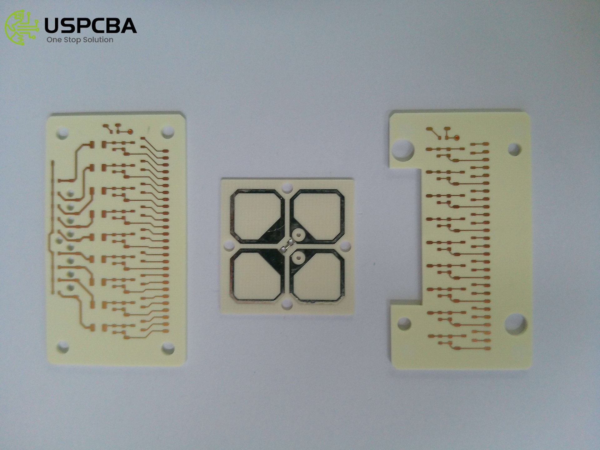
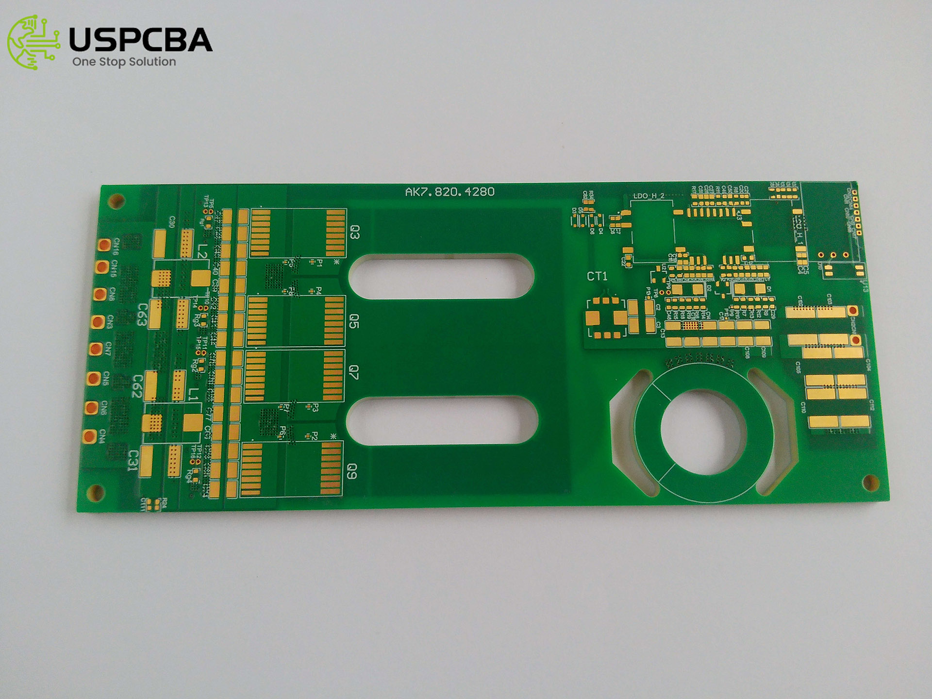
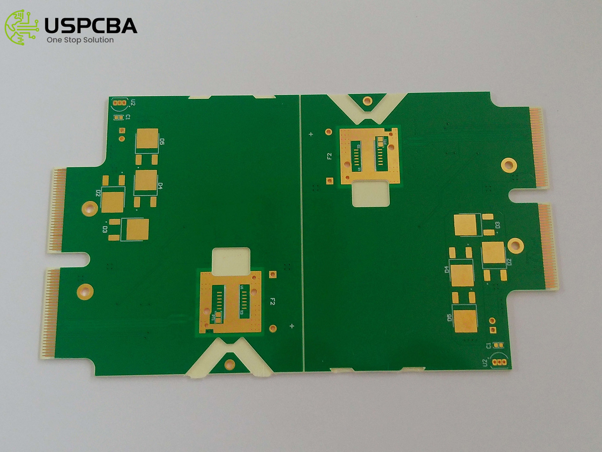
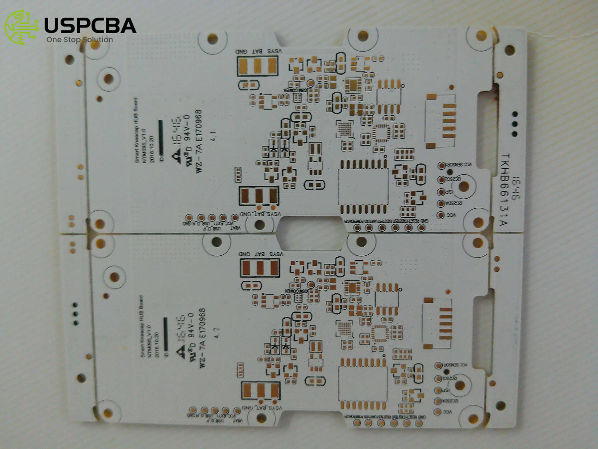
CEM-1 PCB material is one of the substrates of the printing circuit board. It is widely used in single-sided PCB, which will greatly reduce design costs.

Application: Consumer electronics field
Characteristic: Min. width/space: 4/4mil, Aspect ratio:12:1
Material: FR4, 94V-0, RoHS
PCB Layer: 6 Layers
Thickness: 1.6mm
Copper thickness: 1oz - 2oz
Surface finished: Immersion gold (2u")
Solder Mask: Green
IPC Standard: IPC 600 Class 2 & Class 3
Testing: AOI Inspection & 100% E-test
REQUEST A QUOTE

CEM-1 CEM-3 – Technical specification

Feature Technical specification
Number of layers 2 ~ 52 layers
Materials FR4, ( 94V-0, Tg 135, Tg 150, Tg 170 )
Solder Mask Color Green, Blue, Black,White, Red, Yellow, Purple, Pink, Grey
Characters White, Yellow, Black, etc.
Board Thickness 0.2mm - 6.0mm
Copper weights (finished) 0.5oz - 6.0oz
Minimum Trace/Space 0.07mm / 0.07mm
Minimum dimensions 5mm x 5mm;
Maximum dimensions 610mm x 600mm
Minimum mechanical drill (PTH) 0.15mm
Minimum laser drill (blind/micro hole) 0.1mm
Surface finished

HASL - Hot air solder leveling
Lead - free HASL - RoHS
ENIG - RoHS
Immersion Silver - RoHS
Immersion Tin - RoHS
Golden finger - RoHS
OSP - RoHS

E-Testing 100% E-Test , Flying Probe Test & Fixture Test
IPC Standard IPC 600 Class 2 & Class 3

Cem-1PCB

Cem-1 PCB is a bit unfamiliar to most people, Cem-1 PCB is one of the substrates of printed circuit boards. It is low grade in the PCB material industry and is only suitable for single-sided PCBs, but it is widely used.

Some would say that technology is advancing so fast now that every electronic device is getting smaller and smaller. Why such a low-grade material can be widely used.

Yes, the technology is getting higher, but the average time, components are also higher, assembling more features, which will allow more designers to use single-sided PCB (Cem-1 material) to control costs.

The single-sided PCB (single-layer PCB) will greatly reduce the design cost, which is the most important reason.

The special feature of this material is that metallization through holes is not possible, therefore, this material can only be used for the production of 1-layer printed circuit boards.